O.K. then - the display routine is in the works. You can already warm up the soldering iron.darkatx wrote:here it is - looks good
Introducing VFLI for VIC-20: 208x256 pixels in 16 colours!
Moderator: Moderators
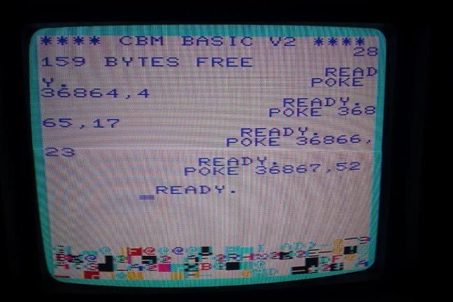

I noticed these are the values I used for "Retina Display" which shows 192x416 interlaced. I came up with these values by using the horizontal and vertical height knobs to squeeze the picture as much as possible on my 1084 and then used the most centered values for the resolution.Mike wrote:Can you confirm that this display window fits neatly in your monitor without cropping the corners?Code: Select all
POKE36864,2
POKE36865,20
POKE36866,24
POKE36867,52
I think from previous discussions it is clear that there is no "perfect" setting that works good on all displays. Each one seems to have a slightly different size, position or cut-off point at the borders. That is probably why Commodore included the thick borders in the first place to fit as much TV-sets as possible.
So, a "perfect" software solution would ask the user to set the screen paramters upon first install and then use these values the rest of the time.
-
Mike

- Herr VC
- Posts: 5134
- Joined: Wed Dec 01, 2004 1:57 pm
- Location: Munich, Germany
- Occupation: electrical engineer
Well spotted.tokra wrote:I noticed these are the values I used for "Retina Display" which shows 192x416 interlaced.
I'm quite aware, that the settings I worked out with darkatx within two iterations might possibly again be cropped on the monitors of other users. The point however is to have a working NTSC VFLI mode available at all as soon as darkatx has conducted the mod.
The target resolution of 168x384i has a similar display window size as used by MINIGRAFIK and should work without any problem on most NTSC monitors.
-
freshlamb

- Vic 20 Dabbler
- Posts: 76
- Joined: Sun Apr 04, 2004 5:38 pm
- Website: http://www.rufnoiz.com
- Location: Prince Albert SK Can
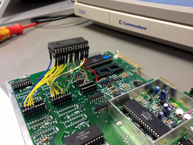
QAPLA!! I have successfully wired up Mikes VFLI mod on an NTSC computer. Mike has also uploaded a NTSC version of the VFLI disk and tools. I wanted to document my progress, so I put up a quick web page here http://www.rufnoiz.com/Vic/vfli.html . I also collected Mikes instructions into a PDF and they are here: http://www.rufnoiz.com/Vic/VFLI.pdf . I hope to do some work with the new VFLI system but I imagine it will be later, when it gets cold here.
K
K
Last edited by freshlamb on Mon Dec 16, 2013 5:04 pm, edited 1 time in total.
-
Mike
- Herr VC
- Posts: 5134
- Joined: Wed Dec 01, 2004 1:57 pm
- Location: Munich, Germany
- Occupation: electrical engineer
The archive can be downloaded here: vfli_ntsc_prototype.zip.freshlamb wrote:Mike has also uploaded a NTSC version of the VFLI disk and tools.
As I wrote earlier, the resolution of 184x208 pixels is intended as stop-gap measure until I find time to implement the 168x384i display routine.
Last edited by Mike on Thu Feb 20, 2014 4:19 pm, edited 1 time in total.
-
Mike
- Herr VC
- Posts: 5134
- Joined: Wed Dec 01, 2004 1:57 pm
- Location: Munich, Germany
- Occupation: electrical engineer
Re: Introducing VFLI for VIC-20: 208x256 pixels in 16 colour
One month ago, I had a short PM exchange with Richardc64 regarding an alternative approach to fill up BLK0. He also brought forward his concerns about the permanent character of the RAM expansion, to quote him, and my replies:
Richardc64 wrote:First, there can never be external 3K.
Mike wrote:That is only a 'problem' if the external 3K comes with some intended extra-function, like a banking scheme (which I've not yet seen thus far), or the possibility to write protect it. The latter is actually the case with FE3, which provides the SJLOAD floppy speeder in that address range, and write-protects it to guard it, well, against writes. With the internal BLK0 expansion that write protection doesn't work anymore, as the internal RAM expansion takes precedence. Nevertheless, the floppy speeder itself continues to work.
Richardc64 wrote:Second, and more significant, IMO, is the possibility of a program that requires an unexpanded Vic and is incompatible with the software method of limiting memory. I don't see any simple way to hardware disable internal 3K.
That being said, I still have to see an example program which requires a +8K or bigger RAM expansion but doesn't anymore work, when the +3K RAM expansion is added to that. Or a program for unexpanded VIC-20, which trips over the extra +3K, when it has been blocked for BASIC use by the POKE/SYS statement above.Mike wrote:Of course it is possible to write a program, which checks for RAM being present in $0400 .. $0FFF (but doesn't use it) and then maliciously decides not to run. I'd consider such cases 'broken by design'.
To date, I have not encountered any program which would even unintentionally fall over the extra RAM, when using the software method of limiting memory (say, with POKE642,16:POKE644,30:POKE648,30:SYS64818). For auto-starting cartridges, you couldn't software-limit the RAM anyway, but screen memory and colour RAM also sit at the same correct address, regardless of unexpanded or +3K expanded RAM.
Conversely, [there are] cartridges like 'Bug Crusher'[, which] *don't* work together with a +8K RAM expansion (using a multi-slot expander), because they still execute parts of the KERNAL reset which puts the screen at $1000, but they then expect it at $1E00. m(
-
Mike
- Herr VC
- Posts: 5134
- Joined: Wed Dec 01, 2004 1:57 pm
- Location: Munich, Germany
- Occupation: electrical engineer
Re: Introducing VFLI for VIC-20: 208x256 pixels in 16 colour
In another thread, Mike wrote:The VIC chip is not able to access *anything* at the expansion port. There's a timing barrier in-between, formed by three 74245 buffer chips. They're necessary, because the 6502 cannot tri-state its address bus.
andIn yet another thread, Vic20-Ian wrote:Ref earlier comments ref tristate:
While you are hacking the hardware, could the tristate buffers be removed by replacing 6502 with the Atari 6502 or the 6510?
"Tri-stating the buses
The 6510 and an Atari version of the 6502 can be tri-stated. 573s have an OC input that takes care of that. The 6510 and the Atari version go into tri-state mode the moment AEC/BE becomes (L). A 573 is active the moment OC is (L). This means an inverter is needed: IC07d.
The R/W has to be tri-stated as well: IC11c, a 125 buffer, takes care of this.
ID signal I123 takes care of enabling IC05, the 573 that outputs the data. IC06c, an OR gate, makes sure that IC05 is tri-stated as well during a tri-state demand from the outside world.
Supporting the 6510
The major difference with the 6502 is the 6-bits onboard I/O port. An added 6526 takes care of that. The 6526 may only be visible at the addresses $0000 and $0001. Two 688s, IC08 and IC09 take care of that. Signal I121 and OR gate IC06a take care of the fact whether the 6526 will be enabled at all or not.
When reading from $0000 or $0001, we must make sure that there is no conflict with IC04, the 573 that reads the data from the outside world. Inverter IC07c and OR gate IC06b take care of that."
http://www.baltissen.org/newhtm/ttl6502.htm
Let's keep the discussion in the thread where it really belongs.Vic20-Ian also wrote:"On the original 400/800 design, a series of tri-state buffers surround the 6502 and
do the job of 'detaching' the 6502.
To lower the chip count on the XL & XE lines, Atari developed a custom version of the 6502 which had the simple
tri-state buffers built-in."
If I understand the article correctly it may be that an Atari XL or XE has a Tristate capable 1.7MHz 6502.
Could this be dropped into the Vic and then remove the tri-state buffers to overcome your problem?
http://www.atarimax.com/freenet/freenet ... cle.php?38
The 6502, together with the three 74245 buffers and a few other ICs in the select logic perform a function, which actually could be perceived similar to the capability of the 6510 to tri-state its address bus, so another bus master can address the memory.
However, all the additional hacks necessary to put a 6510 in place of the 6502 in the VIC-20 would presumably result in something quite resembling another well known computer, only it would be using VIA instead of CIAs (and at another address), would 'lack' the SID, and of course keep the VIC-I.
Anyway, what's the point in hacking around the mainboard, just so external memory could be read by VIC-I, if there's a straightforward solution? Namely, putting 8K RAM in place where it can be accessed by the VIC, instead of the 'original' 5K RAM, thus lifting a restriction on the mainboard which has been put into the design just by accident.
Actually, in the meantime I came up with an even simpler solution than what I described here 3 and a half years ago: it replaces the four 6116 2Kx8 SRAM chips with a single 6264 8Kx8 SRAM, and dispenses with UC4 and U13 alltogether - they are not anymore needed! That's the alternate solution, that RichardC64 also discussed with me over PM.
In the end it all boils down whether there is any interest by other people to keep the discussion up. If there's no live discussion, people shouldn't wonder when improvements ultimately are kept under the rug.
Re: Introducing VFLI for VIC-20: 208x256 pixels in 16 colour
Mike, if you read the post before replying you will see I was highlighting an Atari version of 6502 that can tri-state as well as 6510.
If you had a Vic with a socketed 6502 and dropped in the Atari 6502 could you quickly remove the tri-state buffers and use the 2k ram ?
That seems to be a nice solution to gain that extra ram.
If you had a Vic with a socketed 6502 and dropped in the Atari 6502 could you quickly remove the tri-state buffers and use the 2k ram ?
That seems to be a nice solution to gain that extra ram.
Vic20-Ian
The best things in life are Vic-20
Upgrade all new gadgets and mobiles to 3583 Bytes Free today! Ready
The best things in life are Vic-20
Upgrade all new gadgets and mobiles to 3583 Bytes Free today! Ready
-
Mike
- Herr VC
- Posts: 5134
- Joined: Wed Dec 01, 2004 1:57 pm
- Location: Munich, Germany
- Occupation: electrical engineer
Re: Introducing VFLI for VIC-20: 208x256 pixels in 16 colour
No.Vic20-Ian wrote:If you had a Vic with a socketed 6502 and dropped in the Atari 6502 could you quickly remove the tri-state buffers and use the 2k ram?
And I *read* your second post, and included it here, because it makes no difference whether you'd try this with the 6510 or the Atari 6502C.
If you had taken the time to read the first page of this thread, you'd have seen that I've put quite some detailed thoughts into the VFLI mod. Witness the resistor network on the 'old' /RAMx signals, which serves double purpose. If it's your ambition to design an alternate solution to provide the VIC-I with 8K RAM at $0000 to $1FFF - go ahead, do it - and post the results when it works.
-
Mike
- Herr VC
- Posts: 5134
- Joined: Wed Dec 01, 2004 1:57 pm
- Location: Munich, Germany
- Occupation: electrical engineer
Re: Introducing VFLI for VIC-20: 208x256 pixels in 16 colour
For the 2-prong mainboard I posted this prototype some time ago:Mike wrote:Actually, in the meantime I came up with an even simpler solution than what I described here 3 and a half years ago: it replaces the four 6116 2Kx8 SRAM chips with a single 6264 8Kx8 SRAM, and dispenses with UC4 and U13 alltogether - they are not anymore needed! That's the alternate solution, that RichardC64 also discussed with me over PM.
A single 6264 8Kx8 SRAM replaces the ten 2114 1Kx4 SRAMs of the original 5K built-in RAM, and UC4. Here's the wiring diagram:
Code: Select all
               6264 8Kx8 SRAM (???)

                  +-----\/-----+
                --|NC       Vcc|---- UC4.16 (+5 V)
 (VA7) UD4.17 ----|A12      /WE|---- UD4.10 (VR/W)
 (VA8) UD4.16 ----|A7       CS2|---- UC4.6  (VA13, G1)
 (VA6) UD4.1  ----|A6        A8|---- UC4.1  (VA10, A)
 (VA5) UD4.2  ----|A5        A9|---- UC4.2  (VA11, B)
 (VA4) UD4.3  ----|A4       A11|---- UC4.3  (VA12, C)
 (VA3) UD4.4  ----|A3       /OE|---- UC4.4  (/BLK0, /G2A)
 (VA0) UD4.5  ----|A2       A10|---- UD4.15 (VA9)
 (VA1) UD4.6  ----|A1      /CS1|---- UC4.4  (/BLK0, /G2A)
 (VA2) UD4.7  ----|A0      I/O8|---- UD4.11 (BD0)
 (BD3) UD4.14 ----|I/O1    I/O7|---- UE4.14 (BD7)
 (BD2) UD4.13 ----|I/O2    I/O6|---- UE4.13 (BD6)
 (BD1) UD4.12 ----|I/O3    I/O5|---- UE4.12 (BD5)
 (GND) UE4.9  ----|Vss     I/O4|---- UE4.11 (BD4)
                  +------------+


                      3x 4K7

(+5 V) UC4.16 ----+---/\/\/\-------- UC4.14 (/RAM1)
                  |
                  +---/\/\/\-------- UC4.13 (/RAM2)
                  |
                  +---/\/\/\-------- UC4.12 (/RAM3)


                       .1 U

                       |  |
(+5 V) ???.14 ---------|  |--------- ???.28 (GND)
| |...
For this variant of the mod to be usable, it would be necessary to replace the wired prototype in the photo above by a PCB which hosts the 6264, the 3 resistors and the capacitor, and which goes into the sockets of UC4, UD4 and UE4. Serious lack of time has though prevented me from doing this.
So I'm putting that info up anyhow. Any takers?

Re: Introducing VFLI for VIC-20: 208x256 pixels in 16 colour
I have thought about a similar approach but with some other chips for my board.
However I don't know how to handle the different versions of the boards.
What is your take on that?
It would however be better to avoid cables.
However I don't know how to handle the different versions of the boards.
What is your take on that?
It would however be better to avoid cables.
Last edited by TLovskog on Tue Mar 03, 2015 5:19 pm, edited 1 time in total.
BR
Thomas Lövskog
Thomas Lövskog
-
Mike
- Herr VC
- Posts: 5134
- Joined: Wed Dec 01, 2004 1:57 pm
- Location: Munich, Germany
- Occupation: electrical engineer
Re: Introducing VFLI for VIC-20: 208x256 pixels in 16 colour
For the CR variant, the VFLI mod surely works as described in the first page of this thread.TLovskog wrote:However I don't know how to handle the different versions of the boards. What is your take on that?
If one were to replace the four 2Kx8 SRAMs by a single 8Kx8 SRAM, as I proposed in my post above we'd have to compare pinouts again:
Code: Select all
       6264 8Kx8 SRAM                  6116 2Kx8 SRAM

       +-----\/-----+
 1 ----|NC       Vcc|---- 28
 2 ----|A12      /WE|---- 27           +-----\/-----+
 3 ----|A7       CS2|---- 26     1 ----|A7       Vcc|---- 24
 4 ----|A6        A8|---- 25     2 ----|A6        A8|---- 23
 5 ----|A5        A9|---- 24     3 ----|A5        A9|---- 22
 6 ----|A4       A11|---- 23     4 ----|A4       /WE|---- 21
 7 ----|A3       /OE|---- 22     5 ----|A3       /OE|---- 20
 8 ----|A2       A10|---- 21     6 ----|A2       A10|---- 19
 9 ----|A1      /CS1|---- 20     7 ----|A1       /CS|---- 18
10 ----|A0      I/O8|---- 19     8 ----|A0      I/O8|---- 17
11 ----|I/O1    I/O7|---- 18     9 ----|I/O1    I/O7|---- 16
12 ----|I/O2    I/O6|---- 17    10 ----|I/O2    I/O6|---- 15
13 ----|I/O3    I/O5|---- 16    11 ----|I/O3    I/O5|---- 14
14 ----|Vss     I/O4|---- 15    12 ----|GND     I/O4|---- 13
+------------+ +------------+By "inserting" the 6264 into the socket of one the original 2K SRAMs so the bottom edges align, we'd get GND/Vss, I/O1 .. I/O8 and A0..A10 completely covered. Because Vcc and /WE will need to be taken from the place where the other 2K SRAM resided, it is more sensible to put the chip into the socket of U15.
The other signals require a different treatment, though:
- /CS1 (Pin 20) and /OE (Pin 22) are bent up, combined, and go to the old place of UC4, Pin 4 - one long wire.
- A11 (Pin 23) is bent up and goes to UC4, Pin 2 - another long wire.
- A12 (Pin 2) is bent up and goes to UC4, Pin 3 - the third long wire.
- CS2 (Pin 26) is bent up and goes to UC4, Pin 6 - the fourth long wire.
- /WE (Pin 27) is bent up and goes to the empty socket of the other 2K SRAM, Pin 21 (right side, 4th from top)
- Finally, Vcc (Pin 28) also is taken from the other empty socket Pin 24 (right side top).
The resistor network for /RAM1..3 is still necessary to handle external RAM expansions in that range correctly (i.e. disable them). The capacitor of the "other" SRAM socket handles the voltage stabilization. It is necessary to check if there is enough clearance to the VIA above.
Instead of just two long wires going from the right to the left over the PCB, we now need four wires. But at least there's no need anymore to piggyback chips. And, in any case, neither trace cuts are necessary, nor the extraction of difficult-to-replace chips (like the character ROM, which isn't always socketed), nor soldering of wires to pins of chips which are still soldered in. And the CR variants even don't require a PCB.
So we have yet another, though untested, variant of the mod. My variant on the initial page has the charme it is tested, works, and has been reproduced at least once, and with success.
Re: Introducing VFLI for VIC-20: 208x256 pixels in 16 colour
Hi Mike,
Think I was not clear enough.
That approach, which I would really go for, means a different PCB with different arrangements of the circuits for different VIC 20 motherboards.
I think there are at least 3 major different boards, but how many where the components are only slightly moved?
That was my intended question.
Think I was not clear enough.
With this I thought you meant a PCB with the components. On secondary or solder side male DIP connectors are placed that plugs directly into the socketed UC4, UD4 and UE4.For this variant of the mod to be usable, it would be necessary to replace the wired prototype in the photo above by a PCB which hosts the 6264, the 3 resistors and the capacitor, and which goes into the sockets of UC4, UD4 and UE4.
That approach, which I would really go for, means a different PCB with different arrangements of the circuits for different VIC 20 motherboards.
I think there are at least 3 major different boards, but how many where the components are only slightly moved?
That was my intended question.
Now that is easy to relate to.Serious lack of time has though prevented me from doing this.
BR
Thomas Lövskog
Thomas Lövskog
-
Mike
- Herr VC
- Posts: 5134
- Joined: Wed Dec 01, 2004 1:57 pm
- Location: Munich, Germany
- Occupation: electrical engineer
Re: Introducing VFLI for VIC-20: 208x256 pixels in 16 colour
Probably, giving your explanation next:TLovskog wrote:Think I was not clear enough.
Exactly. On the 2-prong VIC-20 (regardless which of the two variants), the approach of stripping UC4 and desoldering the now useless internal 5K does leave one with no good place to put a 6264 into. Wimoos, for example, piggybacked 6 of the 2114 SRAMs, and routed /RAM1 to /RAM3 to the 6 new chips. Yet another way to do the mod. By plugging into UC4, UD4 and UE4, a PCB gets all necessary signals without any additional wiring.With this I thought you meant a PCB with the components. On secondary or solder side male DIP connectors are placed that plugs directly into the socketed UC4, UD4 and UE4.
I know about your approach of using the character ROM. All necessary signals are also there, but you need to disable the internal RAM by breaking traces on the mainboard. Did you have that in mind, or something else?That approach, which I would really go for, means a different PCB with different arrangements of the circuits for different VIC 20 motherboards.
Are there any examples to single out that hitch?I think there are at least 3 major different boards, but how many where the components are only slightly moved?
I would rather expect, in most cases the components would remain at their place for any big board revision, and maybe some of the traces being slightly rerouted. For example, early CR boards feature a wire soldered to a shrink wrapped resistor going from pin Y of the expansion port for Audio In to the video/sound circuitry - that was soon integrated as trace on the mainboard.
On the more common 2-prong mainboard, I once measured a distance of 16.5 mm between the bottom pins of UC4 and the top pins of UD4, and a distance of 10.1 .. 10.2 mm between the bottom pins of UD4 and the top pins of UE4. Both measurements translate to 6.5/10 and 4/10 of an inch, respectively (with 1/10 of an inch being the standard DIL pin spacing), indicating the chips had been placed on a grid.
Of course, if there are any bigger deviations outside of bearable tolerances (say, 0.1 mm), then any pre-fabricated PCB going into more than one socket is going to fail. That should go without saying.
Re: Introducing VFLI for VIC-20: 208x256 pixels in 16 colour
Well. The reason to go for the ROM was that I, at the time, thought it would be easier to add wires / break traces than to de-solder ICs. I also thought more character ROMs where socketed. I suppose that was only the case with foreign character sets.I know about your approach of using the character ROM. All necessary signals are also there, but you need to disable the internal RAM by breaking traces on the mainboard. Did you have that in mind, or something else?
Another approach then to get nearly the same signals is to have a PCB that plugs into socketed UC4, UD4, UE4, as well as UC5 and UE1. The additional two "ports" would give me access to the color ram and the whole address decoding logic. Making it possible to add RAM at BLK1-3 and 5. Well actually also 6 and 7.
The only missing signals is IRQ which I had in mind for raster interrupt.
BR
Thomas Lövskog
Thomas Lövskog