Thanks, I've added it to my VIC documentation!
(mod: this is the follow-up discussion split off from the original sticky post in the Programming section!)
VIC-20 Memory Layout (follow-up discussion)
Moderator: Moderators

-
Commodorianen
- Vic 20 Drifter
- Posts: 22
- Joined: Fri Jun 02, 2017 11:56 am
- Location: Sweden
Re: VIC-20 Memory Layout (follow-up discussion)
Yes, very good, thank you!
Re: VIC-20 Memory Layout (follow-up discussion)
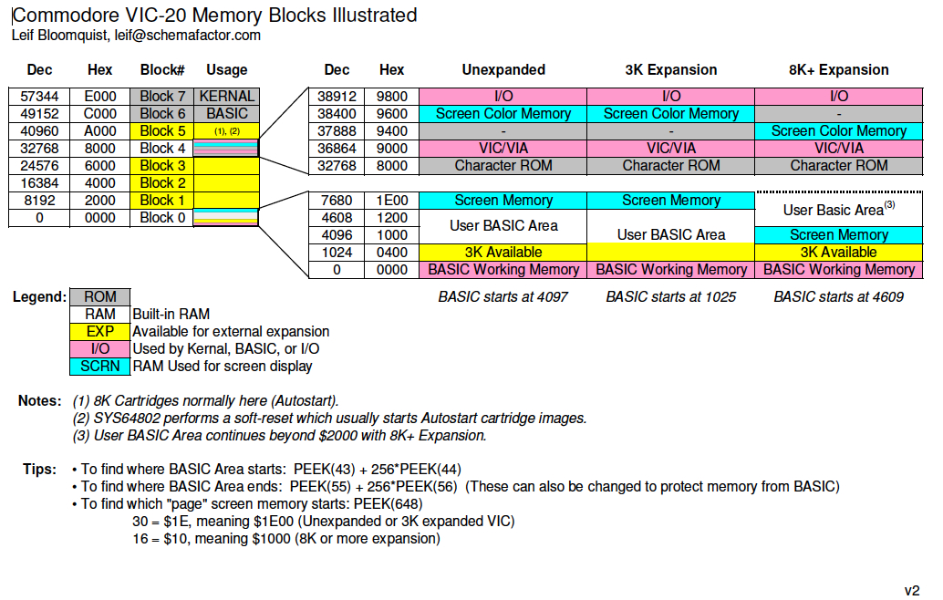
I combined a couple sources to come up with this unified 6565 memory map.
Edit: Updated to include VIA and VIC chip corrections.
Edit: Updated to include VIA and VIC chip corrections.
Code: Select all
                 VIC-20 6560 Memory Map
                    by RevCurtisP
        +---------------------------------------+
        | 6560 = VIC Chip Decoded Address       |
        | Scrn = Screen Memory Location         |
        |        Reg 5 Hi Nybble + Reg 2 Hi Bit |
        | CH   = Character Memory Location      |
        |        Register 5 Low Nybble          |
        | 6502 = 6502 Decoded Address           |
        +---------------------------------------+

+-------+------+----+-------+----------------------------+
|  6565 | Scrn | CR |  6502 | Description                |
+-------+------+----+-------+----------------------------+
| $0000 | $0 0 | $0 | $8000 | Business Gfx Character ROM |
| $0200 | $0 1 |    | $8200 |                            |
| $0400 | $1 0 | $1 | $8400 | Reversed Business Gfx ROM  |
| $0600 | $1 1 |    | $8600 |                            |
| $0800 | $2 0 | $2 | $8800 | Upper/Lower Character ROM  |
| $0A00 | $2 1 |    | $8A00 |                            |
| $0C00 | $3 0 | $3 | $8C00 | Reversed Upper/Lower ROM   |
| $0E00 | $3 1 |    | $8E00 |                            |
+-------+------+----+-------+----------------------------+
| ----- | ---- | -- | $9000 | VIC and VIA Chips¹         |
| ----- | ---- |    | $9200 |                            |
| ----- | ---- | -- | $9400 | Color RAM 0²               |
| ----- | ---- |    | $9600 | Color RAM 1²               |
| ----- | ---- | -- | $9800 | I/O 2 Cartridge            |
| ----- | ---- |    | $9A00 |                            |
| ----- | ---- | -- | $9C00 | I/O 3 Cartridge            |
| ----- | ---- |    | $9E00 |                            |
+-------+------+----+-------+----------------------------+
| $2000 | $8 0 | $8 | $0000 | System RAM                 |
| $2200 | $8 1 |    | $0200 |                            |
| ----- | ---- | -- | $0400 | 3k Expansion RAM           |
| ----- | ---- |    | $0600 |                            |
| ----- | ---- | -- | $0800 |                            |
| ----- | ---- |    | $0A00 |                            |
| ----- | ---- | -- | $0C00 |                            |
| ----- | ---- |    | $0E00 |                            |
+-------+------+----+-------+----------------------------+
| $3000 | $C 0 | $C | $1000 | System RAM                 |
| $3200 | $C 1 |    | $1200 |                            |
| $3400 | $D 0 | $D | $1400 |                            |
| $3600 | $D 1 |    | $1600 |                            |
| $3800 | $E 0 | $E | $1800 |                            |
| $3A00 | $E 1 |    | $1A00 |                            |
| $3C00 | $F 0 | $F | $1C00 |                            |
| $3E00 | $F 1 |    | $1E00 |                            |
+-------+-----------+-------+----------------------------+

1. The VIAs get their select signals from an address
   decoding IC which is exclusively connected to the
   CPU CAx address bus. They put their data on the BDx
   data bus though, while being read.

2. While the VIC has its turn, color RAM is disconnected
   from the lower half of the BDx data bus. Instead, the
   color RAM data is read in parallel to the text screen
   data over four extra pins (VD8..VD11) of the VIC chip.
Last edited by CurtisP on Sat Mar 17, 2018 12:25 pm, edited 1 time in total.
-
Mike

- Herr VC
- Posts: 5130
- Joined: Wed Dec 01, 2004 1:57 pm
- Location: Munich, Germany
- Occupation: electrical engineer
Re: VIC-20 Memory Layout (follow-up discussion)
Nice! VIC can't read its own registers, or the VIA registers *), or the colour RAM **) for text screen and character data, though.
Therefore, this part of the table:
Greetings,
Michael
*) The VIAs get their select signals from an address decoding IC which is exclusively connected to the CPU CAx address bus. They put their data on the BDx data bus though, while being read.
**) while the VIC has its turn, the colour RAM is disconnected from the lower half of the BDx data bus. Instead, the colour RAM data is read in parallel to the text screen data over four extra data pins (VD8..VD11) of the VIC chip.
Therefore, this part of the table:
should read:CurtisP wrote:Code: Select all
+-------+------+----+-------+----------------------------+
| $1000 | $4 0 | $4 | $9000 | VIC and VIA Chips          |
| $1200 | $4 1 |    | $9200 |                            |
| $1400 | $5 0 | $5 | $9400 | Color RAM 0                |
| $1600 | $5 1 |    | $9600 | Color RAM 1                |
| ----- | ---- | -- | $9800 | I/O 2 Cartridge            |
| ----- | ---- |    | $9A00 |                            |
| ----- | ---- | -- | $9C00 | I/O 3 Cartridge            |
| ----- | ---- |    | $9E00 |                            |
+-------+------+----+-------+----------------------------+
Code: Select all
+-------+------+----+-------+----------------------------+
| ----- | ---- | -- | $9000 | VIC and VIA Chips          |
| ----- | ---- |    | $9200 |                            |
| ----- | ---- | -- | $9400 | Color RAM 0                |
| ----- | ---- |    | $9600 | Color RAM 1                |
| ----- | ---- | -- | $9800 | I/O 2 Cartridge            |
| ----- | ---- |    | $9A00 |                            |
| ----- | ---- | -- | $9C00 | I/O 3 Cartridge            |
| ----- | ---- |    | $9E00 |                            |
+-------+------+----+-------+----------------------------+Michael
*) The VIAs get their select signals from an address decoding IC which is exclusively connected to the CPU CAx address bus. They put their data on the BDx data bus though, while being read.
**) while the VIC has its turn, the colour RAM is disconnected from the lower half of the BDx data bus. Instead, the colour RAM data is read in parallel to the text screen data over four extra data pins (VD8..VD11) of the VIC chip.
Re: VIC-20 Memory Layout (follow-up discussion)
So the 6502 can read/write them, but the ViC-20 can't. I'll update my document. Thanks.Mike wrote:Nice! VIC can't read its own registers, or the VIA registers *), or the colour RAM **) for text screen and character data, though.
Re: VIC-20 Memory Layout (follow-up discussion)
Is this why the VIC-20 doesn't hav "bad lines" like the C64?Mike wrote: while the VIC has its turn, the colour RAM is disconnected from the lower half of the BDx data bus. Instead, the colour RAM data is read in parallel to the text screen data over four extra data pins (VD8..VD11) of the VIC chip.
Re: VIC-20 Memory Layout (follow-up discussion)
I also came up with this mapping of the Screen and Character Memory register bits to memory address as seen by the 6502.
Building these tables gave me a deeper understanding of the relationship between the VIC chip and 6502 addressing.
I see this is explained textually in the article at http://sleepingelephant.com/denial/wiki ... nology_VIC but this visual made it a lot clearer to me.
Code: Select all
VIC Register 9002 E-------
             9005 ABCDFGHI

6502 Address  High Byte Low Byte
Screen Memory !A00BCDE0 00000000
Character ROM !F00GHI00 00000000

Note: A and F only are inverted.I see this is explained textually in the article at http://sleepingelephant.com/denial/wiki ... nology_VIC but this visual made it a lot clearer to me.
-
Mike
- Herr VC
- Posts: 5130
- Joined: Wed Dec 01, 2004 1:57 pm
- Location: Munich, Germany
- Occupation: electrical engineer
Re: VIC-20 Memory Layout (follow-up discussion)
No. Actually, the VIC-II in the C64 reads out the colour RAM (it's an extra 1Kx4 SRAM) in quite the same way over those extra 4 data lines. Both machines have effectively the same memory bandwidth - the memory is accessed with 2 MHz, with CPU and Video chip taking turns each microsecond. On the VIC-20, 8 pixels take 2 microseconds to display. That is enough time to *always* fetch text screen (and colour!) and character data and still allow the CPU access in-between.CurtisP wrote:Is this why the VIC-20 doesn't hav "bad lines" like the C64?
On the C64 though, 8 pixels are displayed in 1 microsecond. At least for the first raster of each text line, the VIC-II needs to stop the CPU so it can utilize the extra bandwidth. While doing this, it also stores away the text screen data in an internal register (40 bytes). For the following 7 rasters of the text line, VIC-II fetches the text screen data from the internal register. The display of sprites and the DRAM refresh eat some more cycles, in the left/right border.
With the 264 series (C16/C116/+4), the situation is even more complex. There, the CPU runs in two speeds, 1.8 MHz in the border and 0.9 MHz in the display area. During the display area, TED and CPU take turns as described above, but in the border, the CPU can utilize the full memory bandwidth. However, TED has no extra data path for colour RAM, i.e. the colour data is stored in normal RAM. This incurs *two* badlines: one in the last raster of the preceding text line to fetch the colour data from normal RAM, and the other one like on the C64 in the first raster of the current text line.
Edit:
This comes because UE8 (one of the 3 bus buffers) defines VA13 := /BLK4. This makes the internal RAM appear at $2000..$23FF and $3000..$3FFF from the view of VIC, as well as the character ROM residing at $0000 (with the convenient wrap-around utilized via POKE 36869,255 that allows the use of UDGs alongside the non-inverse upper-case charset). VIC reacts to register accesses whenever $10xx is put on the VA bus. Without the inversion of VA13, VIC would also appear at $1000 for the CPU - a rather unlucky place.Code: Select all
Note: A and F only are inverted.
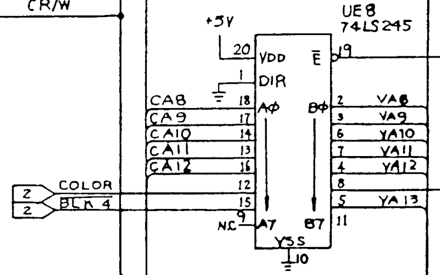
(taken from the schematic of the CR mainboard, and slightly edited for clarity. The address bus buffers, when enabled, have their DIR input pin set so the direction is always from CPU (left) to VIC (right). See pins 15 and 5.)
Re: VIC-20 Memory Layout (follow-up discussion)
It seems to me that the VIC-20 was hacked together by mad geniuses, but that seems to be the norm in that era.
Re: VIC-20 Memory Layout (follow-up discussion)
I found it handy to make an Excel spreadsheet with 256 very skinny rows and 256 very skinny columns. That way you can literally see every single byte at once (with a bit of scrolling), color individual cells, etc.. Additional columns on the sides and top with a very small font size can calculate & display addresses in decimal, hex & binary all at the same time  You can also make grids of 22x23 for screen mockups.
Actually I think it would be very educational if a program existed with a display like this, that was also an assembler. As you coded each opcode, you could see the cells in the grid being colored in. It would give you a better intuition for how much memory is consumed by code and data. It could even have branches in a different color with little arrows pointing to the branch target address, etc.
Actually I think it would be very educational if a program existed with a display like this, that was also an assembler. As you coded each opcode, you could see the cells in the grid being colored in. It would give you a better intuition for how much memory is consumed by code and data. It could even have branches in a different color with little arrows pointing to the branch target address, etc.
-
The Geek on Skates
- Vic 20 Drifter
- Posts: 33
- Joined: Fri Jul 12, 2019 6:11 am
- Website: http://www.geekonskates.com
- Occupation: Code Monkey
Re: VIC-20 Memory Layout (follow-up discussion)
Man, thanks for all your hard work on this, everyone! I've been dealing with a WEIRD graphics bug / code generally getting overwritten whenever I compile my code for 8k+. In fact that was a big part of why the game I'm building is currently for the unexpanded VIC; but I'm sure the more I look at all these great diagrams and stuff, I'll eventually figure it out. Up till now I've been looking at it as a cc65 problem (config files etc.) but I think the real cause might be the differences in where things get moved when you add RAM. Regardless, thanks again!