Soliciting VIC-20 Internal memory expansion ideas

Modding and Technical Issues

Moderator: Moderators

User avatar
Mike
Herr VC
Posts: 4842
Joined: Wed Dec 01, 2004 1:57 pm
Location: Munich, Germany
Occupation: electrical engineer

Re: Soliciting VIC-20 Internal memory expansion ideas

Post by Mike »

brain wrote:@cd:ramcheck.d64
Please disable any kind of OS extensions like JiffyDOS and re-run the RAM check with a standard KERNAL and BASIC ROM only.

The RAM check reinitialises both BASIC and KERNAL vectors at $03xx, and it also utilises the tape buffer to hold machine code - this likely collides with workspace used by OS extensions.

Generally, you'd want to run such tests with as few unknowns as possible.
DrVeryEvil
Vic 20 Amateur
Posts: 69
Joined: Thu Jul 23, 2015 5:11 pm
Location: Lansing, MI, USA
Occupation: Data Analyst

Re: Soliciting VIC-20 Internal memory expansion ideas

Post by DrVeryEvil »

I have built this before. I had two banks of 4K for the character rom space, using a full 8K. All the signals come from the character rom socket. By using banking for the kernal and basic roms, I was able to convert the "Fast Assembler" for the 64, to the VIC and it works great. I had a control register mapped at $9200, breaking down the decoder for IO to make more space, and compatible with the stock VIC. My design works just like on the 64. Good luck with your project.
DrVeryEvil
Vic 20 Amateur
Posts: 69
Joined: Thu Jul 23, 2015 5:11 pm
Location: Lansing, MI, USA
Occupation: Data Analyst

Re: Soliciting VIC-20 Internal memory expansion ideas

Post by DrVeryEvil »

20200422_103837.jpg
20200422_103846[1].jpg
I have had success making a plug-in board with RAM on it, that goes into the socket for the character rom.
User avatar
Mike
Herr VC
Posts: 4842
Joined: Wed Dec 01, 2004 1:57 pm
Location: Munich, Germany
Occupation: electrical engineer

Re: Soliciting VIC-20 Internal memory expansion ideas

Post by Mike »

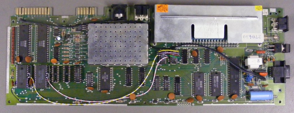
Here's how the internal +3K RAM expansion looked in my VIC-20 before I completed the VFLI mod:

Image

The 4K7 pull-ups on the original /RAMx signals are on the soldering side of the mainboard.
DrVeryEvil wrote:Good luck with your project.
Looks more to me like Jim's project is in hibernation mode since mid-February, for whatever reasons.
DrVeryEvil
Vic 20 Amateur
Posts: 69
Joined: Thu Jul 23, 2015 5:11 pm
Location: Lansing, MI, USA
Occupation: Data Analyst

Re: Soliciting VIC-20 Internal memory expansion ideas

Post by DrVeryEvil »

Mike wrote:The 4K7 pull-ups on the original /RAMx signals are on the soldering side of the mainboard.
I don't have any pull-ups for this since the RAMx signals from the decoder are still connected to the 74LS133.
User avatar
Mike
Herr VC
Posts: 4842
Joined: Wed Dec 01, 2004 1:57 pm
Location: Munich, Germany
Occupation: electrical engineer

Re: Soliciting VIC-20 Internal memory expansion ideas

Post by Mike »

DrVeryEvil wrote:I don't have any pull-ups for this since the RAMx signals from the decoder are still connected to the 74LS133.
You should really be more specific in how you actually made that thing work as supposed!
in another thread, DrVeryEvil wrote:With my internal 3K, I pulled a simple trick by taking the select lines, pins 1,2, & 3, and separating them from the VA bus and tying them to ground. RAM0, then controls the 8K ram chip that replaces the 5K that was put there originally. Since $0000-$03ff is available to the VIC already, the whole 8K is also made available.
See here: http://sleepingelephant.com/ipw-web/bul ... php?t=7750.

Well, that actually ensures the high levels on all the original /RAMx signals, for the 74LS133 and for the cartridge port. Those are details you shouldn't miss out when writing about such topics. :roll:
brain
Vic 20 Nerd
Posts: 538
Joined: Sun Jul 04, 2004 10:12 pm

Re: Soliciting VIC-20 Internal memory expansion ideas

Post by brain »

Mike wrote: Wed Apr 22, 2020 11:14 am Looks more to me like Jim's project is in hibernation mode since mid-February, for whatever reasons.
I wired up the new board, and quickly got the CPU RAM expansion working. But, when I tried to bridge over the VIC bus, it all went south. I have to take some time to redo my "buffer board" that sits in between the VIC and the expansion (I had it running with the previous boards, but it won't fit on this new design) and I've just been procrastinating.

In essence, the buffer board takes in the VIC address lines and data lines, the address and data lines from the VIC socket, and the address and data lines from the new RAM expansion. It then plays traffic cop on the lines depending on clock cycle state (high = cpu/ram, low = VIC socket), so I can determine the issue (it's some sort of timing issue I have to solve...). Once I can determine the issue, I can wean the design off the buffer board, and then I should be ready again for testing.

So, not really hibernating, just procrastinating. I need a good weekend to work on it, and one has not presented itself yet.

Jim
brain
Vic 20 Nerd
Posts: 538
Joined: Sun Jul 04, 2004 10:12 pm

Re: Soliciting VIC-20 Internal memory expansion ideas

Post by brain »

Last night and today saw some time to wire up the buffer board.

Image

Last night, I got all the address and data lines going through the one CPLD (half the time, address direction is one way, half the other, data is always input on VIC cycle portion, direction depends on r/w line for cpu cycle. That is all working.

Today, I moved the databus over (CPU portion, so all CPU access is bypassing the VIC-20 motherboard. But, address lines are having some issue. Trying to track it down.
DrVeryEvil
Vic 20 Amateur
Posts: 69
Joined: Thu Jul 23, 2015 5:11 pm
Location: Lansing, MI, USA
Occupation: Data Analyst

Re: Soliciting VIC-20 Internal memory expansion ideas

Post by DrVeryEvil »

Brian says, address lines are having some issue. Trying to track it down.
You may want to check out the address buffers and VA13. The CA13 does match up with VA13 on the schematic, it uses BLK4 to pass CA13 to VA13.
What are you trying to do with the CPLD? I've tried replacing the buffers, LS245's, with a CPLD without any luck when it came to the upper address buffer, and I've determined it's not worth it to pursue the answer since it wouldn't save any pins, it just moves the buffer inputs and outputs to the CPLD and you still need to hook them up in the VIC mother board.
User avatar
Mike
Herr VC
Posts: 4842
Joined: Wed Dec 01, 2004 1:57 pm
Location: Munich, Germany
Occupation: electrical engineer

Re: Soliciting VIC-20 Internal memory expansion ideas

Post by Mike »

DrVeryEvil wrote:The CA13 does match up with VA13 on the schematic, it uses BLK4 to pass CA13 to VA13.
Read this as: "CA13 does NOT match up with VA13 on the schematic, /BLK4 instead is passed to VA13."
brain
Vic 20 Nerd
Posts: 538
Joined: Sun Jul 04, 2004 10:12 pm

Re: Soliciting VIC-20 Internal memory expansion ideas

Post by brain »

DrVeryEvil wrote: Mon May 04, 2020 7:06 am
Brian says, address lines are having some issue. Trying to track it down.
You may want to check out the address buffers and VA13. The CA13 does match up with VA13 on the schematic, it uses BLK4 to pass CA13 to VA13.
What are you trying to do with the CPLD? I've tried replacing the buffers, LS245's, with a CPLD without any luck when it came to the upper address buffer, and I've determined it's not worth it to pursue the answer since it wouldn't save any pins, it just moves the buffer inputs and outputs to the CPLD and you still need to hook them up in the VIC mother board.
Yep, got va13 covered.

Code: Select all

always @(*)
// this translates the VIC address into the larger 16 bit memory map.
// I put the ROMs in the main memory map where the CPU would see them
// so, I need to convert when the VIC accesses.
begin
   case (address_vic[13:12])
      0: address_vic_out = 4'b1000;
      1: address_vic_out = 4'b1001;
      2: address_vic_out = 4'b0000;
      3: address_vic_out = 4'b0001;
   endcase
end

assign va13 =                    ((address_cpu[15:13] == 4) ? 0 : 1);

assign address_vic =             (phi0_bus ? {va13, address_cpu[12:0]} : 14'bz); // place bus address on vic lines on phi0
assign address_mem =             (phi0_bus ? {3'b0, address_cpu} : {3'b0, address_vic_out , address_vic[11:0]});
I'll do some more work on it tonight or tomorrow night. I have it all hooked up the large logic analyzer now.

Jim
User avatar
Mike
Herr VC
Posts: 4842
Joined: Wed Dec 01, 2004 1:57 pm
Location: Munich, Germany
Occupation: electrical engineer

Re: Soliciting VIC-20 Internal memory expansion ideas

Post by Mike »

Jim,

I think the fundamental misunderstanding on your side is, that VIC addresses on the VA bus somehow are translated to CPU addresses on the CA bus. The reverse is the case. VIC has its own 14 bit address space, and selects itself there (during PΘ2=1 or, equivalently on the VIC-20, during SΘ2=1) for its registers when there's an address of $10xx on the VA bus.

Seen from the CPU, the address bus buffers map all CPU accesses within $8000..$9FFF to $0000..$1FFF on the VA bus (which consequently shows the VIC registers at $90xx for the CPU), and *all* others (i.e. CPU address in $0000..$7FFF or $A000..$FFFF) to $2000..$3FFF on the VA bus! Now except where those CPU addresses with /BLK4 = 1 happen to be in $0000..$03FF and $1000..$1FFF, the '133 in conjunction with the data bus '245 blocks all these accesses, and neither are any of the internal RAMs or VIAs or VIC on the VA bus selected. This is the situation on a stock VIC-20.

For the VFLI mod, I had to remove the 'blockade' of the data bus for $0400..$0FFF effected by the '133 by tying high the original /RAMx signals, with the intended side effect that it also silences external +3K RAM expansions.

I still don't see any merit in allowing VIC access to a full 64K range - or giving it access to the expansion port even! - when the price to pay is that its registers need to be mapped to other places in CPU space. Exactly 0% of existing software (including the KERNAL) will be able to cope with this.

Regards,

Michael

P.S. just in case this has somehow be missed: the 6502 does not tri-state its address bus during SΘ2=0. That's exactly the reason the '245 address bus buffers are there at all.
brain
Vic 20 Nerd
Posts: 538
Joined: Sun Jul 04, 2004 10:12 pm

Re: Soliciting VIC-20 Internal memory expansion ideas

Post by brain »

Mike wrote: Mon May 04, 2020 1:49 pm Jim,

I think the fundamental misunderstanding on your side is, that VIC addresses on the VA bus somehow are translated to CPU addresses on the CA bus. The reverse is the case. VIC has its own 14 bit address space, and selects itself there (during PΘ2=1 or, equivalently on the VIC-20, during SΘ2=1) for its registers when there's an address of $10xx on the VA bus.
I am not sure I am misunderstanding, but I might be mis-communicating what my project is doing. I agree on the VIC, the CA bus is translated into the VA bus, not the other way around, but in my design, I have placed all the RAM and ROM on my main PCB, which is is separated from both the VA and CA busses. As a result, I have chosen to make the "MA" bus look like the map the CPU sees, and this means that I have to convert the VA bus to the BA bus (which is essentially the same as the CA bus in mapping for now). There is also the pins of the CPU, which we can call UA for now.
Seen from the CPU, the address bus buffers map all CPU accesses within $8000..$9FFF to $0000..$1FFF on the VA bus (which consequently shows the VIC registers at $90xx for the CPU), and *all* others (i.e. CPU address in $0000..$7FFF or $A000..$FFFF) to $2000..$3FFF on the VA bus! Now except where those CPU addresses with /BLK4 = 1 happen to be in $0000..$03FF and $1000..$1FFF, the '133 in conjunction with the data bus '245 blocks all these accesses, and neither are any of the internal RAMs or VIAs or VIC on the VA bus selected. This is the situation on a stock VIC-20.
Or, conversely, in my design, if VA wants to see $0000-$1fff of memory, it needs to be directed to $8000=$9fff in the MA memory map.
For the VFLI mod, I had to remove the 'blockade' of the data bus for $0400..$0FFF effected by the '133 by tying high the original /RAMx signals, with the intended side effect that it also silences external +3K RAM expansions.
Understood. I plan to continue to support RAM signals in my design, but optionally turn them off so one can use them with the VIC-I.
I still don't see any merit in allowing VIC access to a full 64K range - or giving it access to the expansion port even! - when the price to pay is that its registers need to be mapped to other places in CPU space. Exactly 0% of existing software (including the KERNAL) will be able to cope with this.
If I get my Verilog working correctly, they won't need to be. The initial goal of the project is to insert the PCBs, pull out all the RAM and ROM from the VIC-20, turn the unit on with stock KERNAL and BASIC, and the unit will function just as before (I know, boring... Why bother :-)). ONce I have that working, then I can work on the rest of my ideas.
Regards,

Michael

P.S. just in case this has somehow be missed: the 6502 does not tri-state its address bus during SΘ2=0. That's exactly the reason the '245 address bus buffers are there at all.
It's good information, though I am aware. In my design, the VA, CA, and my new 'MA' bus are isolated with the equivalent of '245s. The rules to connect them are:
  • During s02 low, tie VA to MA and map VIC address requests to main memory read requests (it's a bit more complicated, since the memory bus is 8 bits and the VIC bus during this phase is 12 bits, but I will cover that later) VA13:12 = 0 -> $8xxx/1->$9xxx/2->0XXX/3->1xxx
  • During s02 high and VIC-I access, tie UA to VA and convert va13
  • During s02 high and any other IO access, map UA to CA
  • During s02 high and RAM read access (for now), tie UA to MA
  • for write, tie UA to MA AND CA, so data gets written to RAM on motherboard
Right now, I have a second CPLD that is doing the following:
  • During so2 low, place VIC-I address on VIC-I socket address lines and place VIC-I socket data lines onto VIC-I data lines (output address, read data from main memory)
  • During s02 high and IO address is in VIC register space, place address value from VIC-I socket onto VIC-I pins and connect VIC-I data pins to VIC-I socket data pins in the direction needed (R/W)
That all works. But, I need to swing the VIC-I from looking at it's own socket for address and data to my PCB. THat is where I am having troubles. I am sure it's Verilog coding error, just need to look at the data.

Jim
User avatar
MCes
Vic 20 Afficionado
Posts: 458
Joined: Fri Jul 24, 2015 1:19 am
Location: Italy

Re: Soliciting VIC-20 Internal memory expansion ideas

Post by MCes »

I haven't read everything, but may be that this memory map representation could help... (VIC MAP)
14-1.jpg
The VIC MAP is not completely perfect, example is "COLOR" area: the 1k-nibble of colour datas are never readable by VIC on BD0..3 data bus, but they will be proposed at VIC on its VD8..11 lines and it will be mirrored covering all VIC addressable area.
"Two things are infinite, the universe and human stupidity, and I am not yet completely sure about the universe." (Albert Einstein)
brain
Vic 20 Nerd
Posts: 538
Joined: Sun Jul 04, 2004 10:12 pm

Re: Soliciting VIC-20 Internal memory expansion ideas

Post by brain »

Debugging got harder, so I finally hooked the unit up to my 16702A logic analyzer:

Image

I was able to get the VIC signals flowing through the "switch" daughtercard I installed, where the signals were simply being buffered by the CPLD from the VIC socket to the VIC IC. But, getting the signals to the main board was not working.
Post Reply