TLovskog wrote:However I don't know how to handle the different versions of the boards. What is your take on that?
For the CR variant, the VFLI mod surely works as described in the first page of this thread.
If one were to replace the four 2Kx8 SRAMs by a single 8Kx8 SRAM, as I proposed in my post above we'd have to compare pinouts again:
Code: Select all
       6264 8Kx8 SRAM                  6116 2Kx8 SRAM

       +-----\/-----+
 1 ----|NC       Vcc|---- 28
 2 ----|A12      /WE|---- 27           +-----\/-----+
 3 ----|A7       CS2|---- 26     1 ----|A7       Vcc|---- 24
 4 ----|A6        A8|---- 25     2 ----|A6        A8|---- 23
 5 ----|A5        A9|---- 24     3 ----|A5        A9|---- 22
 6 ----|A4       A11|---- 23     4 ----|A4       /WE|---- 21
 7 ----|A3       /OE|---- 22     5 ----|A3       /OE|---- 20
 8 ----|A2       A10|---- 21     6 ----|A2       A10|---- 19
 9 ----|A1      /CS1|---- 20     7 ----|A1       /CS|---- 18
10 ----|A0      I/O8|---- 19     8 ----|A0      I/O8|---- 17
11 ----|I/O1    I/O7|---- 18     9 ----|I/O1    I/O7|---- 16
12 ----|I/O2    I/O6|---- 17    10 ----|I/O2    I/O6|---- 15
13 ----|I/O3    I/O5|---- 16    11 ----|I/O3    I/O5|---- 14
14 ----|Vss     I/O4|---- 15    12 ----|GND     I/O4|---- 13
       +------------+                  +------------+
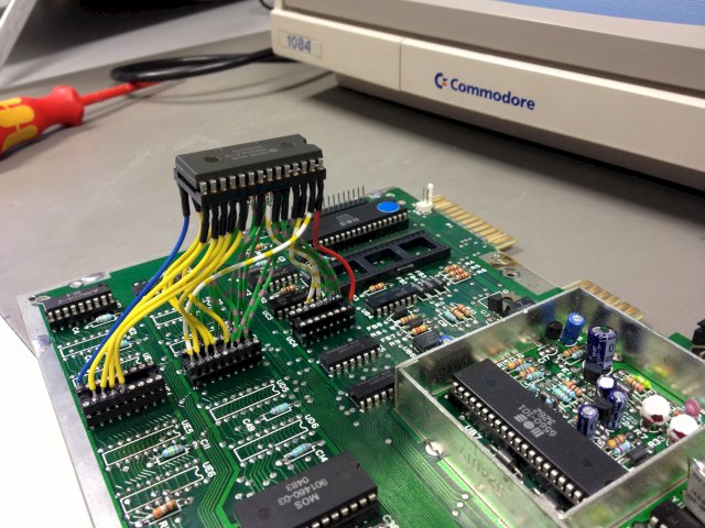
First, U13, UC4 and the original 5K RAM are removed similarly to the original VFLI mod for the VIC-20 CR.
By "inserting" the 6264 into the socket of one the original 2K SRAMs so the bottom edges align, we'd get GND/Vss, I/O1 .. I/O8 and A0..A10 completely covered. Because Vcc and /WE will need to be taken from the place where the other 2K SRAM resided, it is more sensible to put the chip into the socket of U15.
The other signals require a different treatment, though:
- /CS1 (Pin 20) and /OE (Pin 22) are bent up, combined, and go to the old place of UC4, Pin 4 - one long wire.
- A11 (Pin 23) is bent up and goes to UC4, Pin 2 - another long wire.
- A12 (Pin 2) is bent up and goes to UC4, Pin 3 - the third long wire.
- CS2 (Pin 26) is bent up and goes to UC4, Pin 6 - the fourth long wire.
- /WE (Pin 27) is bent up and goes to the empty socket of the other 2K SRAM, Pin 21 (right side, 4th from top)
- Finally, Vcc (Pin 28) also is taken from the other empty socket Pin 24 (right side top).
The resistor network for /RAM1..3 is still necessary to handle external RAM expansions in that range correctly (i.e. disable them). The capacitor of the "other" SRAM socket handles the voltage stabilization. It is necessary to check if there is enough clearance to the VIA above.
Instead of just two long wires going from the right to the left over the PCB, we now need four wires. But at least there's no need anymore to piggyback chips. And, in any case, neither trace cuts are necessary, nor the extraction of difficult-to-replace chips (like the character ROM, which isn't always socketed), nor soldering of wires to pins of chips which are still soldered in. And the CR variants even don't require a PCB.
So we have yet another, though untested, variant of the mod. My variant on the initial page has the charme it is tested, works, and has been reproduced at least once, and with success.